 είσοδος μελών
Διαθέσιμο
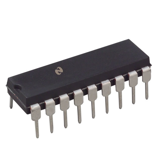
18 - Bit Stage Static Shift Register.
Description
CD4006B types are composed of 4 separate shift register sections: two sections of four stages and two sections of five stages with an output tap at the fourth stage. Each section has an independent single-rail data path.
A common clock signal is used for all stages. Data are shifted to the next stage on negative-going transitions of the clock. Through appropriate connections of inputs and outputs, multiple register sections of 4, 5, 8, and 9 stages or single register sections of 10, 12, 13, 14, 16, 17 and 18 stages can be implemented using one CD4006B package. Longer shift register sections can be assembled by using more than one CD4006B.
To facilitate cascading stages when clock rise and fall times are slow, an optional output (D1+4') that is delayed one-half clock-cycle, is provided (see Truth Table for Output from Term.
Features
- Fully static operation
- Shifting rates up to 12 MHz @ 10 V (typ.)
- Permanent register storage with clock line high or low - no information recirculation required
- 100% tested for quiescent current at 20 V
- Standardized, symmetrical output characteristics
- 5-V, 10-V, and 15-V parametric ratings
- Maximum input current of 1 uA at 18 V over full package-temperature range; 100 nA at 18 V and 25°C
- Noise margin (full package-temperature range) =
1 V at VDD = 5 V
2 V at VDD = 10 V
2.5 V at VDD = 15 V - Meets all requirements of JEDEC Tentative Standard No. 13B, "Standard Specifications for Description of 'B' series CMOS Devices"
- Applications
- Serial shift registers
- Frequency division
- Time delay circuits
- προσφορές (39)
- OKW-Κουτιά- κουμπιά (2748)
- ROLEC (5)
- TEKO - BOXES (944)
- ITALTRONIC (457)
- KRADEX (413)
- MASZCZYK (333)
- Fischer Elektronik-CASES (470)
- Fischer Elektronik-ΨΥΚΤΡΕΣ (1833)
- Fischer - Connectors - Spacers (84)
- IoT Products (16)
- P.C.B - Prototype / Spray (19)
- Active Comp./ Sensors (1497)
- Passive Comp./ ΠΑΘΗΤΙΚΑ (828)
- LCD, LED, OPTO.. (180)
- Connectors,Jack,adapt (426)
- Electromechanical (167)
- ΚΟΛΛΗΣΗ / ΚΟΛΛΗΤΗΡΙΑ (4)
- Buzzers (10)
- ΕΡΓΑΛΕΙΑ / ΟΡΓΑΝΑ (112)
- ΚΑΛΩΔΙΑ (149)
- ΑΞΕΣΟΥΑΡ LAPTOP (16)
- ΠΕΡΙΦΕΡΕΙΑΚΑ Η/Υ & LAPTOP (24)
- ΔΙΚΤΥΑΚΑ (63)
- ΤΡΟΦ/ΚΑ, INVERTER,UPS (164)
- Μπαταρίες / ENERGY (29)
- ΗΛΕΚΤΡΟΛΟΓΙΚΑ-ΣΥΣΤ.ΑΣΦ/ΑΣ (39)
- ΕΙΚΟΝΑ & ΗΧΟΣ (20)
- GPS / SMARTPHONE / TABLETS (2)
- ΠΡΟΣΦΟΡΕΣ ΟΛΟΚΛΗΡΩΜΕΝΩΝ (8)